Summary
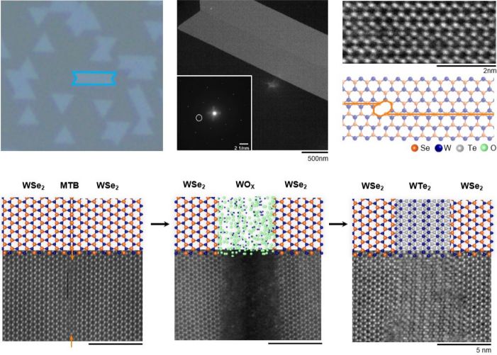
In the world of silicon semiconductors, the process of creating transistors and similar structures involves various rounds of modifications and additions in order to create the requisite functional layers. A less involved approach would simply create these structures in-situ, with research the past years having focused on transition-metal dichalcogenide (TMDC) monolayers to do exactly this. Recently [Seok Young Min] et al. reported (paywalled, Phys.org summary) on creating transistors in-situ in a tungsten ditelluride (WTe2) monolayer. By selectively changing parts of the top layer into tungsten oxide (WOx) as an insulator and other sections into n-type WS2 and p-type WSe2 the researchers were able to create functional MOSFETs, without the normally requisite grafting on of different materials. An obvious advantage of this is that this can be done at an atomic scale, potentially achieving densities significantly higher than with industry standard silicon semiconductor technology. WTe2 is not the only TMDC that could be viable here, of course, with other researchers investigating the use of MoSe2 for a similar purpose, as in this research by [N. Lu] et al. from 2014. This being the creation of 2D semiconductors, referring to the thin layers of these monolayer TMDCs, along with potentially other materials such as graphene. Please be kind and respectful to help make the comments section excellent. (Comment Policy)