LACED: Peeling Back PCB Layers With Chemical Etching and a Laser
1 min read
Summary
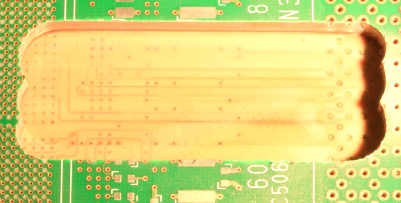
In a novel project, Italian developer Lorentio Brodeso has used chemicals and a 5 Watt diode engraving laser to remove layers from the multi-layered Printed Circuit Boards (PCBs) that are ubiquitous in modern electronic devices.
Whilst the process retains the usual tidy-up issues of chemical etching, it gives greater control, as the laser only targets the solder mask, leaving the copper alone.
The developer has made the process accessible too, as the whole setup costs less than €200.
Brodeso highlights that this approach allows for higher levels of detail to be seen on a multi-layer PCB, and that the method is more precise than mechanical CNC milling.
This “dissecting” technique could be helpful in reverse engineering of electronic devices to ascertain their workings or to create a clone product, and it can also be applied to analyse a legacy PCB to see the routing of different layers.