Summary
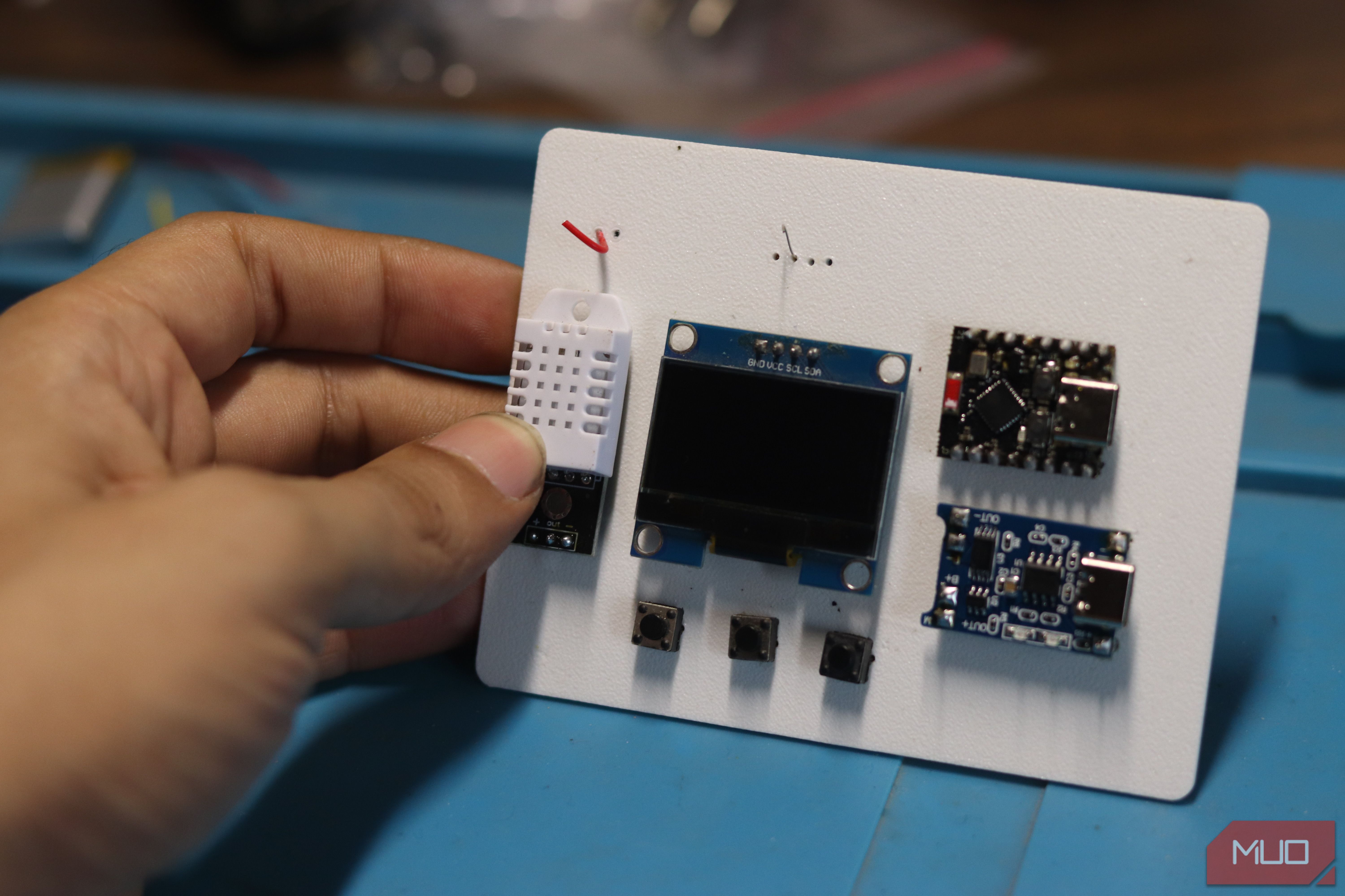
I’m constantly building new smart devices for my house or working on electronics projects that revolve around building circuits. Now breadboards are fine for prototyping, but they’re not exactly great for deployment. Soldering components on a perfboard gives you a more permanent solution, but the wiring is a mess. What I wanted were custom PCBs that I could just drop components into, solder them, and use in proper enclosures. But even the fastest PCB manufacturers can take a week to get these PCBs to your door — a time frame that can be cut down to hours with your 3D printer. Turning your printer into a PCB fab Additive where traditional PCBs are subtractive The idea sounds gimmicky at first, but it makes sense once you break it down. Traditional PCB manufacturing is subtractive. You start with a single piece of copper-clad fiberglass and etch away anything you don’t need. A 3D printed circuit board does the opposite. It adds material where you need it, raising plastic traces which you can then make conductive. The workflow starts exactly like any other traditional PCB. You first do a schematic capture and PCB layout in KiCad, just like you would for a regular PCB. The difference is that you’d want thicker traces than traditional PCBs so you can later raise or recess them and add copper tape or conductive ink to make them conduct electricity. Once you’re finished routing, instead of exporting a Gerber file and sending it off to a manufacturer, you export a STEP file instead and bring it into a 3D modeling program like Fusion 360 or FreeCAD. This is where you clean up the geometry and remove any components you don’t need. You’ll also need to raise (or recess) the traces a couple of millimeters, giving you enough surface area to work with once the board comes off your printer. Then export it as an STL, send it to your slicer, and print out the PCB. You might need to tweak your slicer settings, such as changing the wall type to Arachne to get better finishes, but that’s about it. Making the plastic conductive Copper tape and a hobby knife do the heavy lifting Your printer isn’t laying down copper; it’s laying down plastic, which means the printed part isn’t conductive by itself. There are a few ways this can be solved. The simplest approach is to raise traces on a board printed in PLA or PETG, then apply copper tape over the raised paths and cut away the excess with a hobby knife so only the trace lines remain conductive. This is incredibly simple to do and remarkably effective for low-current signal work. Another, more involved option is to use actual conductive filament or conductive ink poured into trenches designed into the model. Conductive filament exists, but they carry significantly higher resistance than copper, so it’s best reserved for low-current signal traces rather than carrying real power. There’s even dedicated software like Electroprint that takes a KiCad netlist and prepares the model for pause-and-fill conductive printing on multi-material setups. Where this beats ordering a board Same-day turnaround beats a week-long wait every time The single biggest win here is speed. A traditional PCB order, even from a fast fab house, typically takes around a week to arrive, while a 3D-printed prototype can be designed, printed, and tested the same day. If you’re debugging a layout mistake, that turnaround difference is huge, since you can catch the error, tweak the KiCad design, and reprint within hours instead of ordering a whole new batch. Another benefit is the cost, especially for one-off or low-volume boards. A single small traditionally manufactured board can run you tens to over $100 once setup fees are factored in for tiny batches. A 3D-printed version mostly costs you filament and a bit of copper tape. That said, this also works against 3D-printed boards when volume is a requirement. In that case, fab houses are significantly cheaper and better for the project. This method works wonderfully for me because most of my circuits are one-off projects built to solve extremely specific problems. Ordering these boards from a traditional PCB manufacturer means I’ll have to order small batches (whether I’ll use them or not), pay higher costs, and wait longer before I even know whether the final product is the right one. There are limitations 0.2mm traces won’t replace a real fab house 3D printing all your circuit boards does come with a few gotchas. First, trace precision on regular 3D printers tops out at around 0.2mm, while professional fabs routinely hit 0.05mm. This means anything dense or fine-pitched like a modern SMD-heavy board is simply out of reach. Multi-layer boards, vias, and plated through holes are possible, but slightly hard to implement. This trick works best for simple, low-component prototypes rather than finished consumer products. Where it genuinely earns a spot in your workflow is early-stage validation: confirming your layout works electrically before you commit to a real order, building one-off enclosures with embedded wiring, or just cleaning up old projects. Treat it as a fast, cheap sanity check that lives alongside your regular PCB process, and a way to create those one-off circuits without breadboards and jumper cables.